Austrian microfabrication specialist UpNano has introduced a new printing technology designed to address one of the key challenges in high-resolution additive manufacturing: balancing precision with productivity. The company’s new 3D Adaptive Resolution (3DAR) technology enables dynamic voxel control during two-photon polymerization (2PP) printing, allowing manufacturers to produce complex freeform structures with optical-grade surface quality while maintaining high throughput.
As demand grows for increasingly sophisticated micro-optical, photonic and semiconductor components, manufacturers are under pressure to produce geometries that are both more complex and more precise. Conventional layer-based fabrication methods often struggle to achieve smooth curved surfaces without sacrificing production speed, creating a persistent trade-off between quality and throughput.
UpNano’s latest development seeks to overcome that limitation by extending the principles of grayscale lithography into full three-dimensional printing.
Dynamic Voxel Control
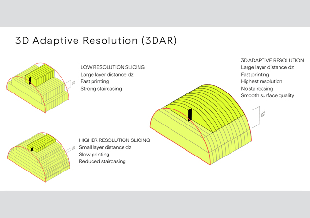
At the heart of the technology is the ability to continuously adjust the dimensions of the printing voxel, the volumetric equivalent of a pixel, in all three spatial directions during fabrication.
UpNano’s Adaptive Resolution technology has been a key feature of its NanoOne printing systems, enabling users to switch between different voxel sizes depending on the level of detail required. Fine voxels can be used for intricate features, while larger voxels accelerate the production of bulk structures.
The newly launched 3DAR technology builds on this approach by allowing the voxel shape to be dynamically adapted to the geometry being printed in real time.
3D Adaptive Resolution gives us dynamic control over the voxel in all three spatial dimensions. We can continuously adapt its shape to the geometry we want to create. This allows us to combine printing speed with the surface quality required particularly for optical and photonic applications,” says Bernhard Küenburg, CEO of UpNano.
By adapting the voxel itself rather than relying solely on thinner layers, 3DAR reduces the staircase effect typically associated with layer-based manufacturing while preserving throughput. The result is the production of complex freeform geometries with smooth surface finishes, an important requirement for next-generation optical and photonic devices.
Targeting Optical and Photonic Applications
The technology has particular relevance for micro-optics and photonics, where surface finish and dimensional accuracy directly influence performance.
UpNano reports that 3DAR can achieve surface roughness values as low as Sq 3nm and shape accuracy below 20nm. The company has also demonstrated the rapid production of complex optical components, including 125µm spiral phase plates fabricated in less than 10 seconds and 7µm aspheric microlenses produced within two to three seconds.
Such capabilities are expected to benefit applications requiring highly customised optical elements and freeform geometries, particularly where traditional fabrication techniques face limitations.
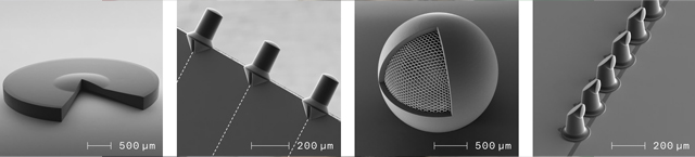
The technology has particular relevance for micro-optics and photonics
Supporting Semiconductor Packaging
Beyond optics manufacturing, UpNano sees significant opportunities in semiconductor packaging and silicon photonics.
A key advantage of 2PP technology is its ability to print directly onto pre-structured substrates. Optical elements such as microlenses and mirrors can be fabricated directly on photonic chips, fibre arrays and chip facets, eliminating a number of alignment and assembly steps.
This capability is becoming increasingly important as the semiconductor industry explores silicon photonics and co-packaged optics to address growing data-transfer requirements.
In AI data centres, where higher computing performance places increasing demands on bandwidth and energy efficiency, optical interconnects are playing an increasingly critical role. Directly printing coupling structures onto chips and optical components could help improve performance while simplifying manufacturing processes.
Moving Toward Industrial Adoption
The launch also reflects UpNano’s ongoing transition from research-focused systems to industrial manufacturing platforms. The company says the first 3DAR-capable systems have already been acquired by an Asian customer, which has expressed interest in deploying additional units. While details remain undisclosed, the early commercial uptake suggests growing industry interest in high-throughput microfabrication technologies capable of producing complex geometries at nanometer-scale precision.
Founded in 2018, UpNano has steadily expanded the capabilities of its NanoOne technology platform, targeting applications ranging from micro-optics and photonics to microfluidics, life sciences and industrial microparts. Its systems offer resolutions below 100nm while supporting structures ranging from sub-micrometer features to centimetre-scale components.
Enabling Next-Generation Microfabrication
As industries such as photonics, semiconductor manufacturing and advanced packaging continue to push the limits of miniaturisation, production technologies must deliver increasingly demanding combinations of accuracy, throughput and design freedom.
With 3DAR, UpNano is positioning its 2PP platform as a solution capable of addressing those requirements, enabling manufacturers to produce complex freeform structures with improved surface quality without compromising productivity.
For applications where optical performance depends on nanometer-level precision, the technology could offer a new route to scaling advanced microfabrication from prototyping to industrial production.